


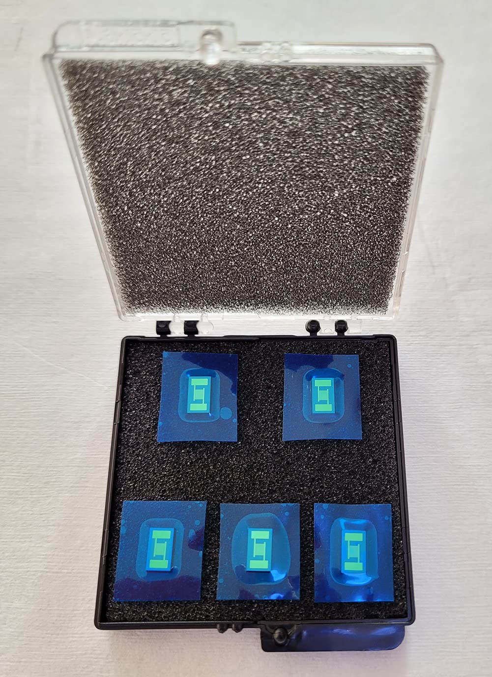
This high precision monocrystalline silicon interdigitated electrode (IDE) is widely used in optical, physical and medical sensors, with reliable performance and stable quality! 1. The substrate: P-type monocrystalline silicon with 300nm thickness of SiO2 on the surface of the silicon wafer. The size of the substrate is 7mm ╳ 4mm ╳ 0.52mm. 2. The conductor layer structure: Cr/Au, the thickness are 30nm and 100nm respectively. 3. The line width: 20μm; The line space: 20μm. Finger Length: 1500μm; Number of interdigitate pairs : 30(60 fingers). 4. The resistance of electrode is more than 100T ohm (room temperature, humidity 64%). The suitable temperature for using is from - 100 degrees Celsius to +400 degrees Celsius. 5. The electrode has large pads, so bonding and soldering are easy. 6. This product can be used as core part of biological, medical and optical sensors. We offer all kinds of interdigitated electrodes, various sizes, various shapes, various substrate, various line spaces and various proceeds (Electroplating, MEMS, Thick film, Printing). Beside of the listing products, We can customize interdigitated electrodes according your needs. Please do not hesitate to contact us, if you have any requirments or questions.
Trustpilot
3 weeks ago
1 day ago